
About 20 years ago, I started working on the design of a microprocessor. The goal was mostly to have fun building a small 32-bit RISC CPU, make it open source, and, most importantly, explain the process behind it. I abandoned the project roughly 18 years ago as I moved on to other things.
This year, I want to bring the project back. Processor design was something we used to learn in univerity at the time, but today it has become much more abstract. Even understanding what actually happens inside a processor is now often treated as a fairly distant concept.
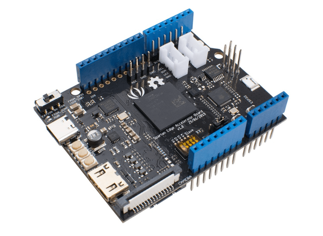
That old work is a good foundation for explaining these ideas again. For that reason, I wanted to refresh the hardware I used years ago to build the processor, which was based on an FPGA that I will discuss in more detail later. Because this is relatively professional hardware, access to FPGA development kits is usually quite expensive. And while it was honestly worth the investment, Seeed Studio has since created a development kit looking like an Arduino, includes an ESP32, and remains much more accessible. It integrates a Xilinx Spartan FPGA. It is not one of the high-end models, but it is still roughly ten times larger than the one I was using around 20 years ago, which makes it a very good fit for this project.
What is an FPGA
An FPGA is a programmable electronic component. But when I say “electronic,” I do not mean a processor that can be programmed with software. I really mean programming the electronics themselves.
In practice, an FPGA contains electronic resources such as logic operators, memory, flip-flops, and similar building blocks. These resources can be programmed to give each of them a specific logical function, and then connected together to create the equivalent of an electronic component with a fully dedicated behavior.
With an FPGA, you can ultimately build almost any advanced electronic component. Compared with an ASIC, it is usually more expensive per unit, but the goal is different. An FPGA makes it possible to build very specific designs in small quantities, which can be far cheaper in the end than designing and manufacturing a custom ASIC at scale. That said, things seem to have evolved quite a lot on that front in recent years.
In any case, what makes an FPGA interesting is that it remains fairly accessible. The truly physical electronics constraints do not directly impact you in the same way, and you can develop electronic circuits almost as if you were developing software.
Of course, the languages are not quite the same. Several options are available. I am more used to VHDL, which is a language used to describe electronic circuits. From a programming perspective, the mindset is also different. You do not have a processor executing instructions sequentially. Instead, you describe electronic components with their own behavior. The result is massively parallel by nature, because each component described in code can operate independently from the others.
Seeed Board
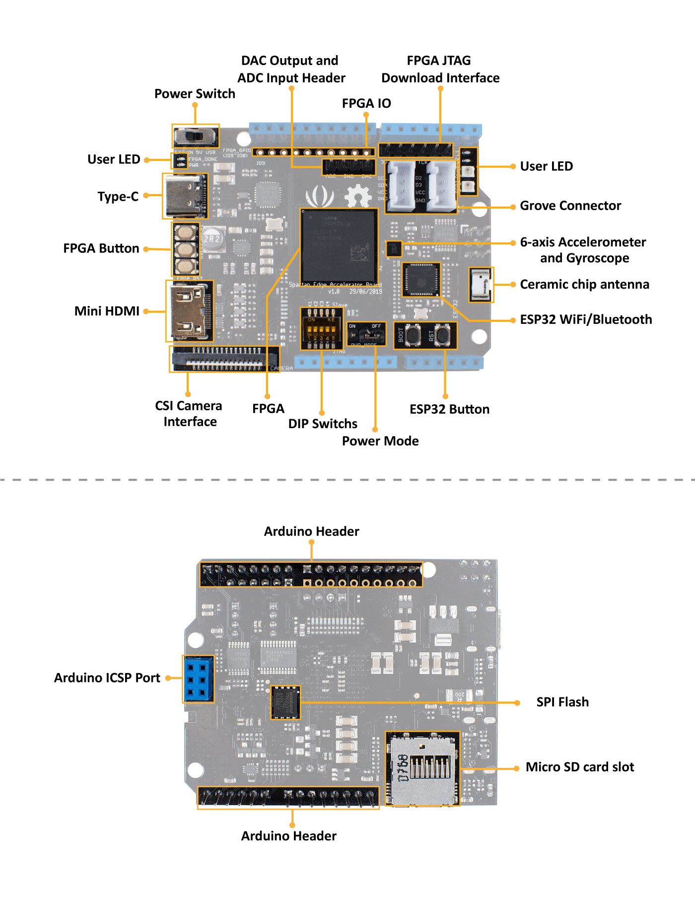
The Seed board uses an Arduino form factor and integrates an ESP32. This ESP32 can act as a companion to the application running on the FPGA, but it can also be used to program the FPGA itself.
The programming flow is based on writing the bitstream file to an SD card, then transferring that file from the SD card to the AMD Spartan component. This is not necessarily the simplest approach, but it avoids the need for a dedicated programming probe from AMD, formerly Xilinx, which can be relatively expensive. In practice, this makes the system quite convenient.
The board also integrates several useful I/Os. For example, it includes buttons connected to the FPGA, as well as LEDs that are also accessible from it. It is also possible to connect an HDMI output and use the FPGA to control video signals. In addition, the system includes a few components that may be useful, such as an accelerometer and SPI flash.
Overall, it is a fairly complete kit for a maker-oriented approach, which fits very well with what I want to do. The Seeed FPGA wiki page already provides a fairly complete guide for installation and first steps. This article builds on that material and complements it.
Integrated AMD Spartan (Spartan-7 XC7S15)
An FPGA is made of logic cells. These logic cells are generally all similar: they contain a set of gates and a set of flip-flops. In the Spartan-7 XC7S15, there are 12,800 logic cells, which makes it a fairly substantial component, although it is still considered a small FPGA compared to what is available on the market today.
In the Spartan-7 family, for example, the number of logic cells can reach several hundred thousand, depending on the specific device reference. Beyond logic cells, another important element inside an FPGA is the flip-flop. Flip-flops are memory elements, but they are not RAM. They are electronic storage components that can operate at the maximum speed of the system. In this device, there are 16k flip-flops elements that can be used for this purpose.
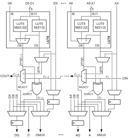
There is also RAM available, up to 150 KB, along with a number of other components that can be accessed in the system depending on what needs to be built.
For the Spartan 7 family, a CLB is a block that contains 2 slices. One slice is composed by 4 LUTs, which defines a logical operation, and 8 flip-flops, which make it possible to store states in the FPGA. To implement logic functions, we use LUTs, or look-up tables. In practice, these are small memory blocks that can take five / six inputs and produce one / two output. For every possible combination of input values, we can define the output we want. This is what allows us to build more complex logic circuits on top of these basic elements.
The FPGA is clocked by an external 100 MHz clock +/- 20ppm.
Installation
Overall, you should follow the tutorial created by Seeed Studio, which is very well written and available at this address.
The idea is to generate a binary from the FPGA development tools and place it on an SD card. This SD card will then be read by the ESP32, which will automatically program the Xilinx device. To make this compilation and deployment flow work, we need to install several components.
Configure Arduino ESP32 to program the fpga
- You need Arduino IDE with ESP32 board support from espressif.
- Select DOIT ESP32 DEVKIT as a board
- Then you need the spartan library containing the code exemple your need to flash. Install it as a zip file. (or you can get my forked version with the modifications included)
The issue is that this library is somewhat outdated, and the spartan-edge-esp32-boot.c file will need to be modified to ensure its content matches the following so that it can compile.
//PULL UP of SD card pins <--- preventing mounting failure due to floating state
//sdmmc_host_pullup_en(1, 4); //Slot: 1 and Bit mode: 4
sdmmc_slot_config_t slot_config = SDMMC_SLOT_CONFIG_DEFAULT();
slot_config.flags |= SDMMC_SLOT_FLAG_INTERNAL_PULLUP;
...
// at the end of the programming function, add
return 0;
- Open the project file 02LoadConfigBitstream from the library example / compile / push it to the ESP32. (switch ESP32 in bootloader mode by pressing boot button when connecting USB power cable)
- You can display the error message on the Arduino console, setting baudrate at 74880. At this step it’s normal to get error message
There is also an alternative solution allowing to flash the Spartan using the SPI flash as a memory to store the bit file and so, transfer the data over the Arduino programming standard. It limits the SDCard in & out but I don’t think it’s really simplify the operation. I’ll investigate other approach, I will let you know as soon as I get the hardware.
Prepare an SDcard to host the fpga binary file
The binary used to configure the Spartan is read from an SD card. This SD card must be prepared beforehand: it needs to be formatted as FAT32 and must contain a configuration file specifying the name of the BIN file to load onto the Spartan at startup.
create a board_config.ini file on the root of the SD Card with the following content
;board infomation
[Board_Info]
board_name = SEA
version = 0,1,0
relese_date = 2019,7,22

;WIFI setting about board
[WIFI_config]
enable = false
ssid = None
password = None

;FTP setting about board
[FTP_config]
enable = false

;setup status about board
[Board_Setup]
boot_on_SDcard = false
overlay_on_boot = quickstart.bit
overlay_actions_comment = always, onbutton, none
overlay_actions = always

;the overlay list
[Overlay_List_Info]
Overlay_List = quickstart.bit
Overlay_Dir = /overlay/
Then create an overlay directory on the SD and copy the quickstart.bit file below into it. Eject the SDCard. Insert it into the board socket and reset the board.
Reset the ESP32 to start programming. You may see a success message after programming. This takes a few seconds.
Once the FPGA is programmed the GREEN led close to the 2 RGB leds may be ON and if you click on one of the two white buttons close to the USB-C connector, the led should switch OFF
Install the FPGA development environment
This part is honestly not the easiest one.
AMD’s development tool, Vivado, feels very old school. It has been a long time since I had that much trouble installing software. First, the TAR archive is 98 GB, so the download takes a while for what is, in practice, an editor and compiler. I assume it also ships with many tools I will never use. Let’s try the network installer…
The bigger issue is that, although Vivado is mostly written in Java, it only runs on x86 processors. I use a Mac, like many people, so that quickly becomes a problem.
I tried several approaches, including running it on an x86 Linux environment through UTM/QEMU emulation. It could have been slow, but still usable. Unfortunately, the installer crashes, probably because something is incompatible, even though the rest of the Linux system works quite well in that environment.
In the end, I used a VDI: a Windows desktop rented monthly from Shadow, an OVH company. I had wanted to test their solution for a while, so this was a good opportunity. It is not exactly the cheapest option, since it costs me roughly the price of the dev kit every month, but for these tests, it remains acceptable. On macOS, I had a keyboard issue with the Shadow environment. I had to use Microsoft Keyboard Layout Creator, or MKLC, to load an Apple keyboard layout. It is still not exactly the real Apple keyboard layout, but at least only the @/# sign and </> keys are inverted. For the rest, it works reasonably well. The process is to install MKLC, which first requires installing the older .NET Framework 3.5. Then you load an existing keyboard layout, choose the Apple French keyboard, go to Project, and build it. This generates an installer file in the Documents folder, which you then run and you can switch keyboard from the bottom bar.
After that, I finally had a usable keyboard, and I could proceed with the AMD Vivado installation. I selected the following items during installation, hoping they were the right ones. The installation requires 71 GB of available disk space, including 20 GB to download the required files.
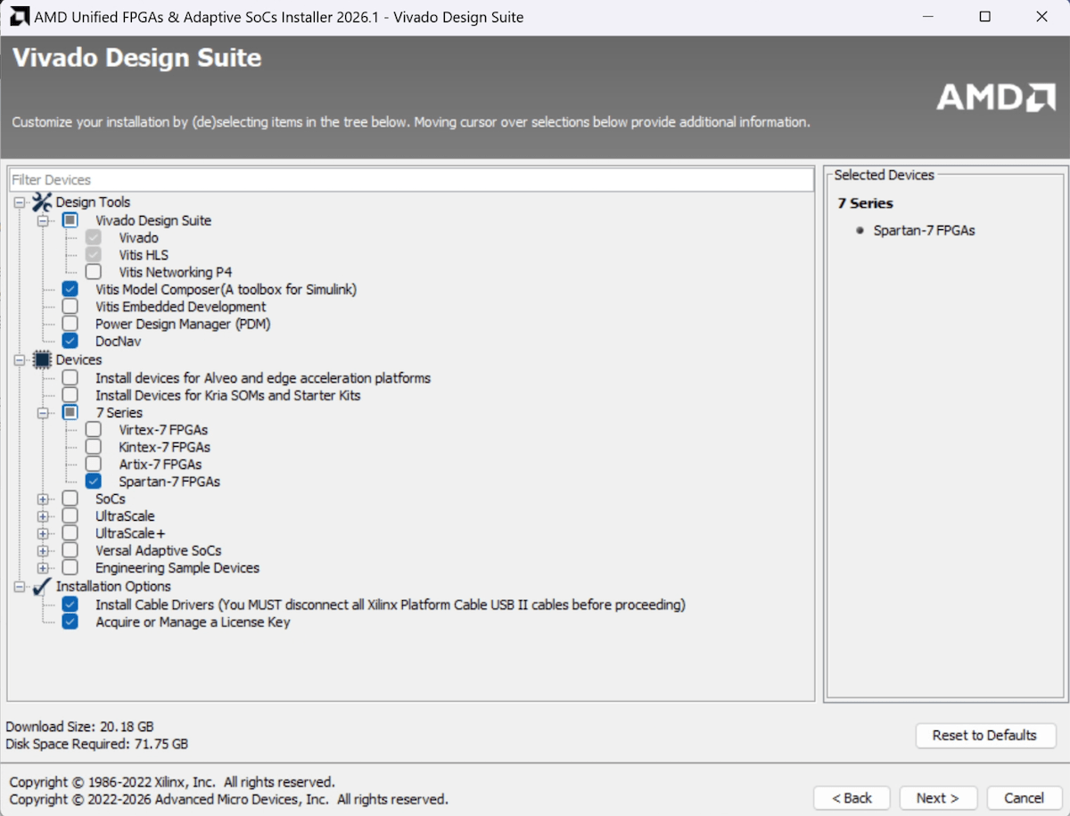
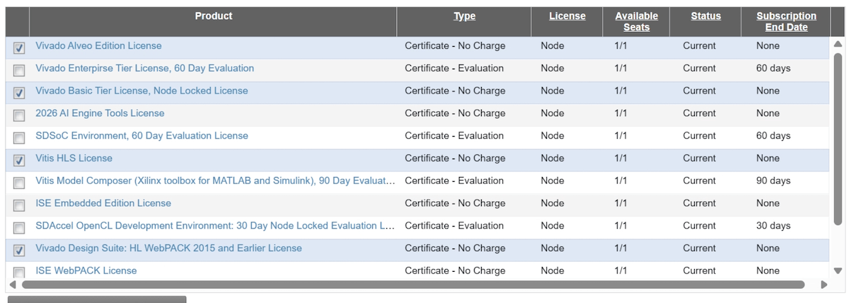
Once the installation is complete, the license screen will appear. Most tools appear to require a license, but these licenses are free, so this should not be an issue.
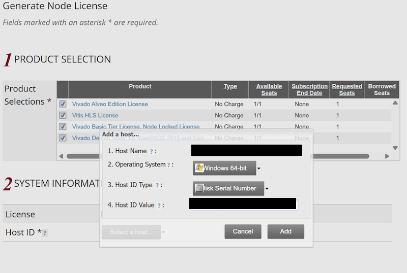
You need to sign in to your AMD account and select the licenses you want to use. Then, you will have to generate a license file using information from the machine, such as the machine name and serial number.
This information can be retrieved from the licensing application through the available menus. Once the license file has been generated, simply download it, and the licenses should normally be active.
Create a first project
We can now launch the Vivado application and create the first project using the icon with the same name.
- Select RTL Project and click Next
- Select no Source file but select VHDL for Language and Simulator Language, click Next
- Do not add constraints, click Next
- Select XC7S17FTGB196-1 device
The project has now been created.
Note : In the past, the Seeed board was natively supported, which meant that Pin configurations could be handled directly. This no longer seems to be the case, which is a bit unfortunate, especially since the board is still accessible.
For my first project, I relied on elements from the Wiki from Seeed, this github tutorial and this Hackster page.
Add PIN DEFINITION (CONSTRAINT FILE)
In the project menu, we can now go to Add Sources and choose to add or create constraints. Create a file like pinmap.xdc. This is how we associate variables with specific pins. Here, we simply map the two ports corresponding to the buttons on the board, as well as the LED that we will be able to turn on. We also map the system clock, which is required for the device to operate properly overall.
set_property IOSTANDARD LVCMOS33 [get_ports {key[0]}]
set_property IOSTANDARD LVCMOS33 [get_ports {key[1]}]
set_property IOSTANDARD LVCMOS33 [get_ports led]
set_property IOSTANDARD LVCMOS33 [get_ports sys_clk]
set_property PACKAGE_PIN C3 [get_ports {key[0]}]
set_property PACKAGE_PIN M4 [get_ports {key[1]}]
set_property PACKAGE_PIN J1 [get_ports led]
set_property PACKAGE_PIN H4 [get_ports sys_clk]
Add the VHDL file
In the Project menu, we will once again select Add Sources, but this time we will Add or Create Design sources. We will create a new file called quick_start.v, with the file type set to VHDL. For the next steps, we will skip the pin definitions and accept the warning popup.
The content is the following one :
library ieee;
use ieee.std_logic_1164.all;

entity quickstart is
    port(
        sys_clk : in std_logic;
        key     : in std_logic_vector(1 downto 0);
        led     : out std_logic
    );
end quickstart;

architecture rtl of quickstart is
    signal flag : std_logic;
begin
    flag <= key(0) and key(1);
    process(sys_clk)
    begin
        if rising_edge(sys_clk) then
            if flag = '1' then
                led <= '1';
            else
                led <= '0';
            end if;
        end if;
    end process;
end rtl;
To understand this program, the idea is actually quite simple. We define a block with inputs and outputs. This is what is described in the port section, where we can find the clock, the two buttons, and the LED.
We then define the processing logic we are interested in. Inside it, there is a signal called flag.
This flag simply performs a logical AND between the two buttons. The result is synchronized with the clock. On the rising edge of the clock, the program checks whether the result of this logical AND is equal to 1. If it is, it sends a 1 to the LED. Otherwise, it sends a 0. As the LED is ON with a 0 and BUTTON gives 0 when click, clicking on one of the button will make the LED OFF.
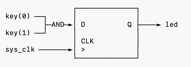
In practice, this means that when both buttons are pressed, the LED turns on or off depending on how it is wired. The code may look quite verbose for something so simple, but this is a fairly standard pattern. In the end, even if we replaced the middle part with a much more complex operation, it would not necessarily require much more code.
Generate the design
In the left sidebar, under the Implementation section, click Run Implementation. This will start the build process, or compilation, for the project. If you see a message indicating that there is no netlist, confirm it. The netlist will be created automatically. The processing progress is shown in the top-right corner of the application window.
After a while, a pop-up will appear indicating that the implementation has completed and offering to Generate a Bitstream. Overall, even for a small circuit like the one we just built, the processing time is particularly long. And of course, like any heavy program of this kind, it will crash from time to time. Don’t worry, that comes with the package.
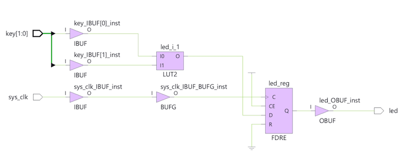
You can take a look at the generated schematic by going to Synthesis and clicking Schematic. This lets you confirm that the overall circuit matches what we intended. Note that the gate performing the AND logic operation is replaced here by a LUT, which implements the same behavior.
Get the bitstream
Once the bitstream has been generated, it is saved in the quickstart.runs directory, under the impl_1 subdirectory, and should be named quickstart.bit. Then you can move the file to the SDCard and flash it on the FPGA.